
A 1000 W accelerator drawing a 700 A load step cannot tolerate more than a 5% core-voltage droop. Divide one by the other and the target impedance works out to 54 microohms. Add more and more decoupling capacitors and the impedance curve still throws up a 1.2 milliohm peak at 225 kHz — 22 times the target. That peak does not sit on any single capacitor's self-resonance. It is created by two capacitor banks in parallel pushing against each other.
The short answer: the anti-resonance peak appears where the bulk capacitor's inductance meets the ceramic bank's capacitance. Its height is the quality factor times the square root of inductance over capacitance, and passive damping alone cannot pull it down to 54 microohms.
54 microohms is a division result, not a selection
The target impedance of a power delivery network (PDN) comes from the allowed voltage droop divided by the load step: Z_target = ΔV / ΔI. That equation is the starting point for the whole PDN design.
Using published parameters: a 0.75 V core rail with a ±5% window gives 37.5 mV, and a 700 A step gives Z_target = 53.6 microohms, rounded to 54 microohms. On a 0.75 V rail that 37.5 mV window is more than twice as tight as the 90 mV window typical of a 1.8 V rail.
That 54 microohms is not a specification for any one capacitor. It is a number the entire chain from VRM to die must hold across 0 to 100 MHz. The low band is held by the VRM loop, the high band by package and on-die capacitance, and the middle band is held by nobody — which is exactly where the anti-resonance peak grows.
The charge budget makes the gap clearer. Holding 700 A for 40 microseconds requires 28 millicoulombs. A 1 millifarad bulk bank can only deliver 37.5 microcoulombs inside a 37.5 mV window — three orders of magnitude short. Board-level capacitors never ride out a step by storing charge; they only hold impedance down until the loop responds. The VRM loop is what actually supplies the charge.
A 48 V intermediate bus with vertical power delivery moves the problem. The input to the 0.75 V stage drops from 48 V to 6 V, duty cycle rises from 1.5% to 12%, minimum on-time no longer limits loop bandwidth, and the 225 kHz peak has a chance to fall inside the loop. The cost is an extra conversion stage and about 1.5 percentage points of end-to-end efficiency.
The peak does not sit on any capacitor
The bulk bank self-resonates at 164 kHz (1880 microfarads, 0.5 nH equivalent inductance). The ceramic bank self-resonates at 71 MHz (1000 microfarads, 5 pH equivalent inductance). Between the two is a flat capacitive impedance that looks peak-free.
The anti-resonance peak is what happens when the two banks meet at the boundary between capacitive and inductive behavior: branch currents run in opposition, and the combined impedance rises instead of falling. The bulk inductance and the ceramic capacitance form a new parallel resonance at f = 1/(2π√(L·C)). Plug in 0.5 nH and 1000 microfarads and you get 225 kHz.
At that frequency the bulk bank is already inductive while the ceramic bank is still capacitive. The two branch currents oppose each other, the impedances cannot cancel, and only loss limits the peak. The peak height is Q·√(L/C). Lossless, √(L/C) is 707 microohms; with a measured Q near 1.7 the peak reaches 1.2 milliohms.
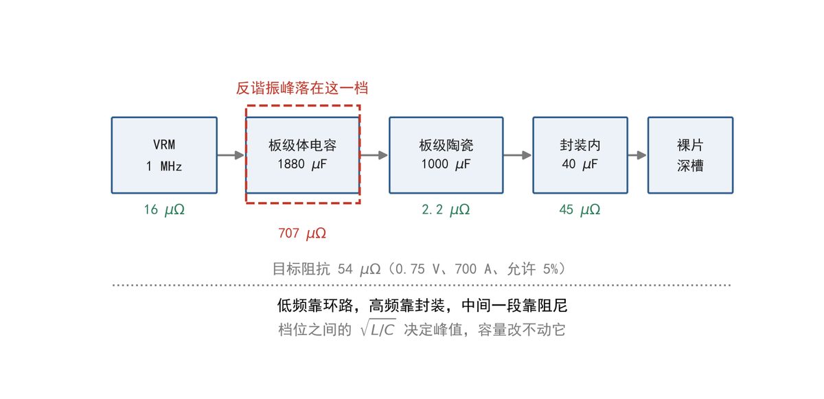
Figure 1: The four power-delivery regions from VRM to die, and the resulting impedance curve (schematic illustration, not a reproduction of the source figure).
A capacitor's self-resonance is not set by its own inductance alone — vias and pads add to it. A single through-hole via with a 0.3 mm drill is roughly 0.3 nH, and it takes 40 in parallel to bring that to 7.5 pH. Combined with 1000 microfarads, self-resonance lands at 1.8 MHz.
Via placement therefore becomes a design variable as important as capacitor part number. Recent published optimization work puts via location and capacitor selection into a single search for precisely this ceiling.
More capacitance does not rescue the curve
Doubling the ceramic bank from 1000 to 2000 microfarads drops √(L/C) from 707 to 500 microohms — a 30% improvement — while the anti-resonance frequency slides down to 159 kHz, further away from the VRM loop.
Inductance is what really sets the peak. Cutting bulk equivalent inductance from 0.5 nH to 0.15 nH drops √(L/C) to 387 microohms and roughly halves the peak, at the cost of eight low-ESL polymer capacitors and about 30% more board area.
To push the peak below 54 microohms, Q would have to fall under 0.08. That is beyond what damping can achieve. The only remaining option is to keep the VRM loop effective at 225 kHz and use loop gain to suppress the peak.
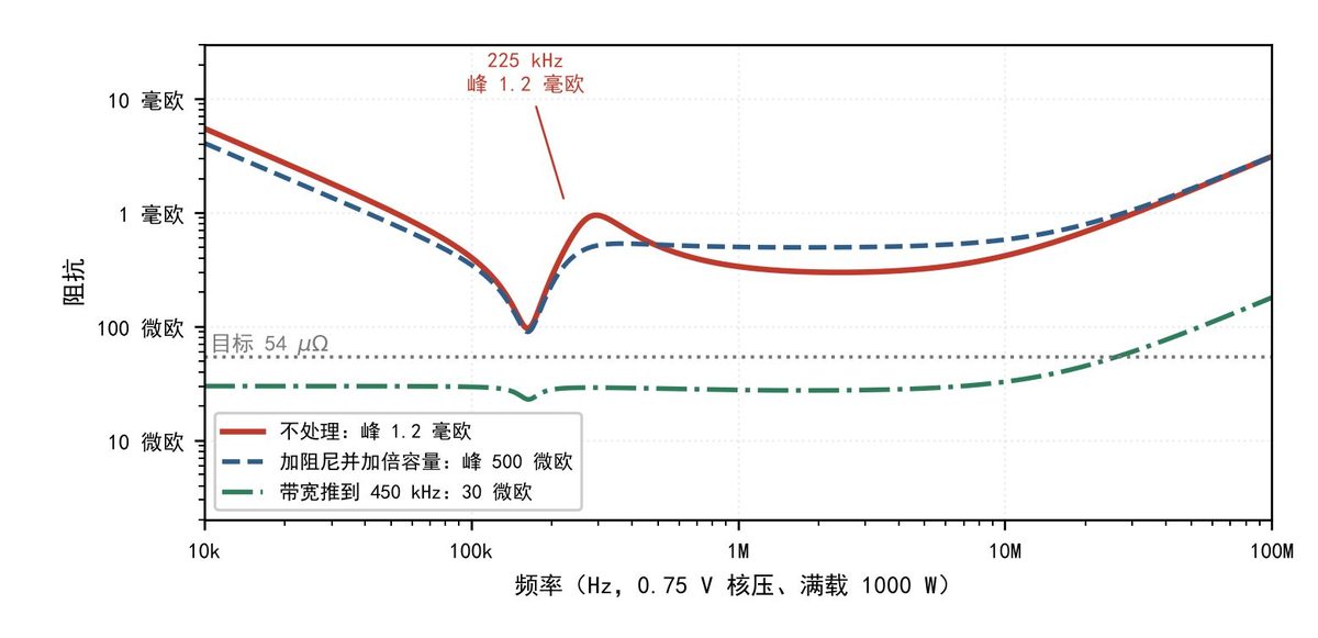
Figure 2: PDN impedance versus frequency under three treatments (redrawn from published parameters, not a reproduction of the source figure).
| Treatment (0.75 V, 700 A, 54 microohm target) | Anti-resonance frequency | Peak impedance | Relative to target | Added loss or area | Verdict (at or below 54 microohms passes) |
| 4 × 470 µF + 100 × 10 µF, untreated | 225 kHz | 1.2 mΩ | 22× | 0 | Fail |
| 4 damping networks, ceramic raised to 2000 µF | 159 kHz | 500 µΩ | 9.3× | 18 W, +30% area | Fail |
| Bulk replaced with 8 low-ESL parts (0.15 nH parallel) | 411 kHz | 390 µΩ | 7.2× | +30% area | Fail |
| VRM bandwidth raised from 200 kHz to 450 kHz | 225 kHz | 30 µΩ | 0.56× | +9 W switching loss | Pass |
| 40 µF deep-trench capacitor added in package | 3.56 MHz | 45 µΩ | 0.83× | +8% package cost | Pass |
Table notes: peak computed as Q·√(L/C) with Q = 1.7; the bandwidth option is the parallel combination of a 30 microohm loop output impedance and the 1.2 milliohm peak; conditions are 25 °C, 1000 W full load, ceramic bank equivalent inductance 5 pH.
Ceramic capacitance falls with temperature and DC bias. An X6S dielectric at 85 °C and rated DC bias loses about 30% of its value, so 1000 microfarads becomes 700 and √(L/C) climbs from 707 to 845 microohms, lifting the peak by about 20%.
When selecting parts, compute Z0 from the capacitance at 85 °C and rated bias, not the 25 °C nominal. On a 0.75 V rail the difference is modest; on rails above 1.2 V it can consume half the margin.
An impedance curve only counts once it is measured on the board. The two-port method uses a vector network analyzer with coaxial probes, and the probe-to-die path must be de-embedded — otherwise everything above 50 MHz is the fixture talking. A 20% gap between simulation and measurement at the anti-resonance peak is common.
Failure case: core voltage drops 9% on a full-load transition
The symptom: a training load jumps from 30% to full, the core rail falls from 0.75 V to 0.68 V — a 9% droop — and the scope captures 225 kHz ringing that recovers after about 40 microseconds.
The cause is that the anti-resonance peak sits outside the VRM loop bandwidth of 200 kHz. Loop gain at 225 kHz is already below 0 dB, so the peak goes unsuppressed and only board-level charge carries the rail through those 40 microseconds.
There are two fixes: push loop bandwidth to 450 kHz so the peak falls inside the loop, or add a 40 microfarad deep-trench capacitor on the package substrate to move the boundary frequency to 3.5 MHz. The first changes the compensation network and sampling rate; the second changes the package.
Analysis: envelope-based capacitor selection breaks at this level
The standard industry approach to PDN design is to draw a target impedance line and keep each capacitor bank's impedance envelope below it. That method does not hold at 54 microohms, because the impedance floor of passive capacitors is set by √(L/C). More capacitance only approaches that value, and once board-level ESL is 5 pH or more, √(L/C) is already in the 100 microohm range. In other words, capacitance cannot buy lower impedance — only inductance can.
That judgment has a clear boundary. When the target impedance is above roughly 500 microohms — a 48 V bus with a 100 A-class load, for example, where the target is around 24 milliohms — the board-level √(L/C) is already below target and envelope-based selection works fine; the problem reduces to a capacitance question. A GPU core rail is not in that region.
Walking through a single 1000 W card
Constraints: 0.75 V core, 1000 W full load, 700 A step, 54 microohm target, 60 × 80 mm board area, 1 MHz VRM switching frequency, 8% cost-increase ceiling.
Three candidates: stacking board capacitors with passive damping, raising VRM bandwidth to 450 kHz, or adding deep-trench capacitance in the package. Their peaks and costs are in the table above; no separate numbers are needed.
The stacking option is the easiest to implement. With 100 × 10 µF parts, four RC damping networks and doubled capacitance, the peak still sits at 500 microohms — 9.3× target — and the core rail would fall to 0.66 V on a full-load step, outside the ±5% window. The package option brings the peak to 45 microohms and passes, at the cost of 8% package cost and a substrate revision.
The chosen path is to raise VRM bandwidth to 450 kHz and add 20 microfarads in the package as a second line of defense. Moving bandwidth from 200 to 450 kHz means shifting the sampling point from mid-switching-period to the valley and pushing the compensation zero from 8 kHz to 20 kHz. Output impedance at 225 kHz drops to 30 microohms, which in parallel with the 1.2 milliohm peak gives 29 microohms.
The costs and risks should be stated plainly: at 450 kHz bandwidth with a 1 MHz switching frequency there are only 2.2 samples per cycle, current-loop phase margin falls from 55° to 38°, and a faster load will ring; switching loss rises by 9 W, costing 0.9 percentage points of card efficiency; and the 20 microfarad deep-trench capacitor takes 6 mm² of substrate, forcing a routing revision.
If the target impedance is below 100 microohms, stop stacking board capacitors. Push VRM bandwidth past the anti-resonance point or add capacitance in the package instead — accepting either 9 W of switching loss or 8% package cost.
What this means for your build
- Compute the target impedance from droop and step current first, then check whether your anti-resonance peak lands inside or outside the VRM loop bandwidth — that single check decides the architecture.
- Treat via placement as a capacitor-selection variable. Parallel via inductance adds directly to ESL and shifts self-resonance; co-optimize the two rather than picking parts in isolation.
- Size ceramic banks at 85 °C and rated DC bias, not 25 °C nominal. A 30% capacitance loss raises the peak by roughly 20%.
- If your target is below 100 microohms, budget for loop-bandwidth changes or in-package capacitance early. Board-level capacitance alone will not close the gap.
- De-embed the probe-to-die path before trusting any measured impedance above 50 MHz, and expect a 20% simulation-to-measurement gap at the peak.
In one line: at 54 microohms, capacitance has no answer — only inductance and loop bandwidth do.
Source: compiled from public web sources.