
Wide-bandgap devices are reshaping the primary side of high-frequency LLC resonant converters, but evaluating their real behavior requires test setups that isolate the variables that matter. This article walks through a hardware platform built to demonstrate a high-frequency LLC design concept and to quantify how an external drain-source capacitor (Cds) affects primary-side dv/dt and power loss. The platform deliberately removes secondary-side influences so that the measurements reflect only the primary-side switching events.
Test platform: a no-load half-bridge equivalent
The schematic is shown in Figure 1. It is a no-load half-bridge (HB) resonant converter that, in terms of dead-time requirements and primary-side switching loss, behaves equivalently to an LLC converter operating near or below resonance. By selecting different inductance values (Lm), different switch currents can be produced, emulating the magnetizing inductance of an isolation transformer in an LLC design. For operation above resonance, the peak magnetizing current (Im_pk) can be raised beyond the normal design range, bringing the effect of load current on the primary switches into consideration. For each device, the gate drive voltage and on/off resistances were adjusted to ensure ZVS at the minimum switch current and a 75 ns dead time. The gate drive parameters were:
- Vgs = 0 V to 12 V
- Rgon = Rgoff = 5 Ω
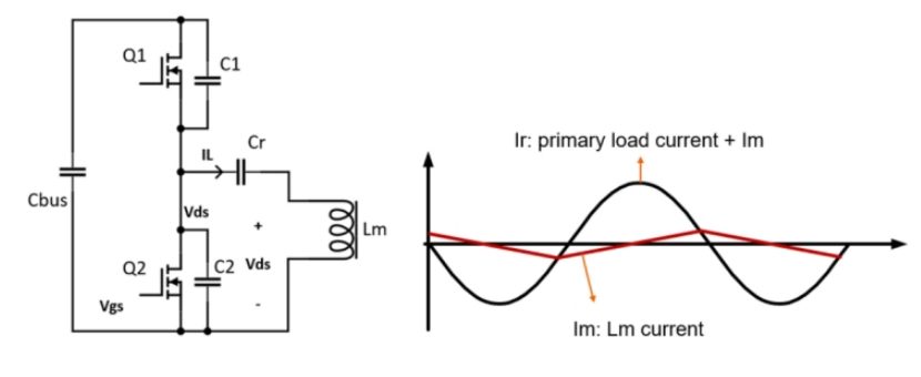
Figure 1. Hardware emulation of a no-load LLC converter. Only the Lm current is considered in this setup.
Baseline waveforms and dv/dt
Figure 2 shows typical CJFET operating waveforms captured at a DC input of 400 V, a dead time of 75 ns, and a switching frequency of approximately 990 kHz. A 5 µH inductor sets the peak magnetizing current (Im_pk) to 10 A. Because the switch current was low, no external Cds was used in this initial test. The waveforms indicate that the CJFET (part number NTBT023N075CJ4, TOLT package) is suitable for the primary side of LLC converters switching up to 1 MHz. With a magnetizing current of about 10 A, ZVS is maintained with ample margin.
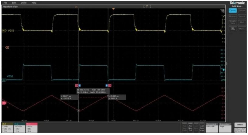
Figure 2. Typical waveforms of the no-load LLC circuit with switch current Isw set to 10 A. Fsw = 990 kHz, Tdt = 75 ns, Vdc = 400 V.
Figure 3 is a zoomed-in view of the turn-off transient from Figure 2. The measured dv/dt of Vds is 31.4 V/ns. With an optimized power-loop inductance and steady-state operation, this dv/dt should not cause switching transient issues.
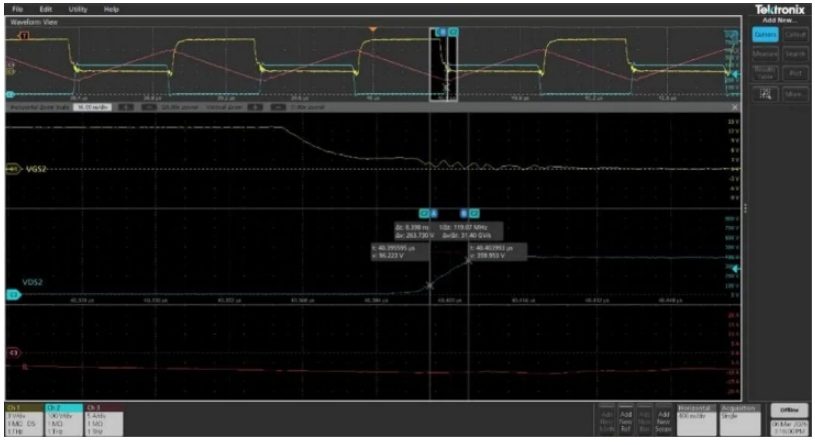
Figure 3. Magnified view of the turn-off transient from Figure 2.
Power loss versus switch current
At a fixed switching frequency, different Lm values produce different switch currents Isw. The total input power delivered to the test circuit was measured for various Isw values, as shown in Figure 4. This total loss includes all losses in the power circuit—inductor winding loss, PCB parasitic resistance (ESR) loss, and device losses (conduction and switching)—but excludes losses caused by load current in an LLC converter. As expected, total loss rises with increasing switch current.
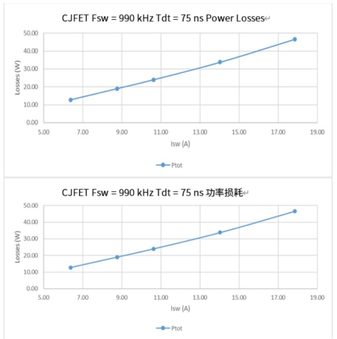
Figure 4. Total power loss versus switch current (Im_pk, peak magnetizing current). Fsw = 990 kHz, Tdt = 75 ns, Vdc = 400 V.
Most of this loss is due to the equivalent series resistance (ESR) of the inductors used, which was in the range of a few hundred milliohms in this test. As with all high-frequency magnetic designs, winding ESR is very significant at 1 MHz. Reducing winding ESR to optimize copper loss remains a major challenge in all high-frequency LLC designs.
Adding a capacitor snubber at 1 MHz
The next test was run in the 1 MHz range with an external snubber capacitor (Cds). Each switch had a 220 pF capacitor in parallel. A 4 µH litz-wire air-core inductor was used in the resonant tank to produce a switch current of about 12 A. Key waveforms are shown in Figure 5. The results show that, despite the added snubber capacitance, the system still had very ample dead-time margin with the slightly higher switch current.
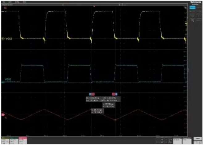
Figure 5. Waveforms with a 220 pF C-snubber across the CJFET, operating at 1 MHz. Switch current Isw = 12 A, Fsw = 990 kHz, Tdt = 75 ns, Vdc = 400 V.
In a third test, the same 4 µH litz-wire inductor was used, and the switching frequency was set to 400 kHz. Vdc was varied from 250 V to 425 V to obtain different switch currents. Total input power and the dv/dt at the switching node were measured.
Figure 6 compares dv/dt with and without the 220 pF Cds at 400 kHz. The 220 pF Cds reduced dv/dt by about half, demonstrating the effectiveness of a snubber capacitor in controlling turn-off dv/dt.
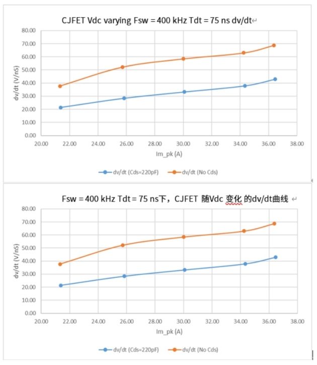
Figure 6. dv/dt comparison with and without external Cds. Vdc = 400 V, Fsw = 400 kHz, Tdt = 75 ns.
Figure 7 compares total power loss with and without the 220 pF Cds. The results show that adding the 220 pF C-snubber reduced total system loss, consistent with the circuit analysis. At low switch current (about 20 A), the difference is not significant; as switch current increases, the difference becomes more pronounced. At a higher switch current (about 36 A), the loss difference can reach about 10 W.
Figure 7. Total power loss comparison with and without external Cds. Vdc = 400 V, Fsw = 400 kHz, Tdt = 75 ns.
Design implications
CJFETs offer high voltage capability, low conduction loss, and fast switching, making them an attractive choice for the primary side of high-voltage, high-frequency LLC resonant converters. In above-resonance operation (higher switch currents), turn-off dv/dt can become excessive, leading to overshoot, ringing, and EMI problems. A parallel capacitor snubber (C-snubber) is a simple, effective, and low-loss way to suppress dv/dt and optimize total loss, and its trade-offs in dead time or switch current are manageable. With proper device selection and circuit layout, overall system efficiency and robustness can both be improved.
What this means for your build
- Plan for dv/dt control early. If your LLC design operates above resonance, include provisions for a C-snubber footprint across the primary switches to manage turn-off dv/dt and mitigate EMI.
- Optimize the power loop. Minimize parasitic inductance in the primary power loop to keep ringing and losses in check, especially when switching at 1 MHz.
- Specify low-ESR magnetics. Winding ESR dominates high-frequency losses; work with your magnetics supplier to select litz wire or other low-ESR constructions.
- Validate ZVS margin. Ensure your gate drive and dead-time settings maintain ZVS across the expected load range, accounting for the added snubber capacitance.
- Coordinate PCB and assembly. Use a fabrication and assembly partner who understands high-frequency layouts, impedance control, and thermal management to realize the full benefit of SiC JFETs.
Source: compiled from public web sources.