
Warpage during reflow soldering is a common and frustrating problem. When a printed circuit board bows or twists as it passes through the oven, it can lead to solder defects such as open joints or tombstoning, where one end of a component lifts off its pad. The root cause is almost always the same: the stress applied to the board exceeds what the material can withstand. When that stress is uneven, or when different areas of the board resist stress differently, the result is bow and twist.
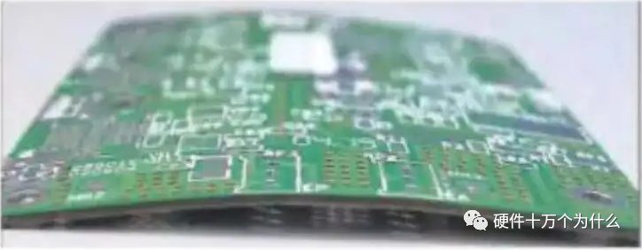
People can bend; PCBs should not. Yet understanding why boards warp is the first step to preventing it.
Where does the stress come from? In reflow soldering, the largest source is temperature. Heat softens the board, distorts it, and combined with the coefficient of thermal expansion (CTE) and the natural expansion and contraction of materials, it creates warpage.
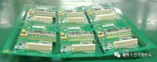
Why some boards warp more than others
Several factors contribute to the severity of warpage. The most common are described below.
1. Uneven copper distribution
Most boards include large copper areas for grounding, and sometimes the Vcc layer also has large copper pours. When these areas are not evenly distributed across the board, heat absorption and dissipation become uneven. The board expands and contracts with temperature, and if different regions expand at different rates, stress builds up and causes deformation. If the board temperature reaches the upper limit of its Tg (glass transition temperature), the material softens and can deform permanently.
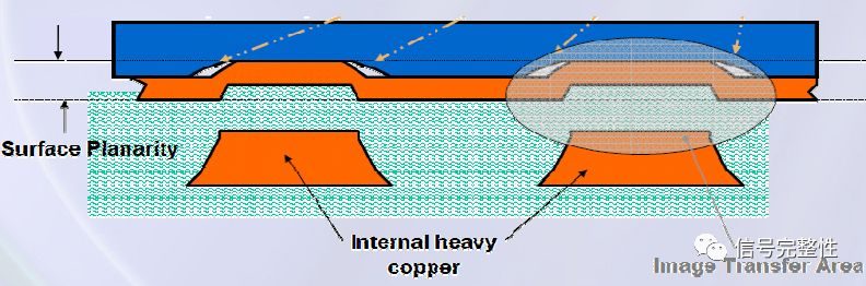
2. Vias restrict expansion and contraction
Modern boards are often multilayer, with vias acting like rivets between layers. These vias can be through holes, blind vias, or buried vias. Where vias exist, they constrain the board's ability to expand and contract, indirectly contributing to warpage.
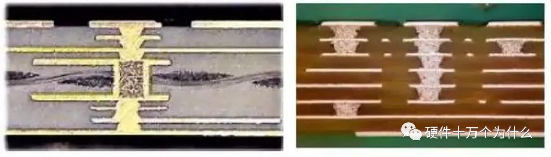
3. Board weight causes sag
Reflow ovens typically use chains to carry boards, supporting them at the two edges. If heavy components are placed on the board, or if the board is large, its own weight can cause the center to sag, leading to warpage.
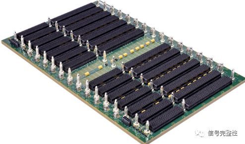
4. V-Cut depth and connecting strips affect panel deformation
V-Cut scoring essentially weakens the panel structure by cutting V-shaped grooves into the board. The V-Cut areas are therefore prone to deformation.
Design and process measures to reduce warpage
To address these causes, consider the following measures during design and production.
1. Reduce thermal stress
Since temperature is the main source of stress, lowering the reflow oven temperature or slowing the heating and cooling rates can significantly reduce warpage. However, be aware of potential side effects such as solder bridging.
2. Use higher-Tg materials
Tg is the temperature at which a material transitions from a glassy to a rubbery state. Materials with lower Tg soften sooner and remain rubbery longer in the oven, leading to greater deformation. Higher-Tg materials can better withstand stress, but they typically cost more.
3. Increase board thickness
To achieve thinner and lighter products, boards are often made at 1.0 mm, 0.8 mm, or even 0.6 mm thick. Keeping such thin boards flat through reflow is challenging. If thinness is not a requirement, using 1.6 mm thickness can greatly reduce the risk of warpage and deformation.
4. Reduce board size and panel count
Because most reflow ovens use chains, larger boards sag under their own weight. Orient the board so that its long edge is parallel to the chain, and reduce the number of boards per panel. During reflow, feeding the board with its narrow edge perpendicular to the direction of travel minimizes sag.
5. Use a reflow carrier or pallet
If the above methods are insufficient, a reflow carrier (pallet) can help. Carriers are typically made of aluminum alloy or synthetic stone that withstands high temperatures. They hold the board flat during heating and cooling, maintaining its dimensions until the board cools below Tg and becomes rigid again. If a single-layer carrier is not enough, a top cover can be added to sandwich the board between two layers. However, carriers are relatively expensive and require manual placement and retrieval.
6. Replace V-Cut with router separation
Since V-Cut weakens the panel structure, avoid V-Cut separation where possible or reduce the V-Cut depth. Routing is an alternative that separates boards without compromising panel strength.
What this means for your build
- Balance copper distribution: Ensure copper pours are as uniform as possible across the board to promote even heating and cooling.
- Consider Tg and thickness: For applications where flatness is critical, specify a higher-Tg material and consider a thicker board (e.g., 1.6 mm) if thinness is not essential.
- Optimize panel design: Reduce board size and panel count, and orient boards so the long edge is parallel to the reflow chain.
- Use carriers when needed: For thin or large boards, a reflow carrier can maintain flatness, but factor in the cost and handling.
- Avoid V-Cut where possible: Choose router separation to maintain panel integrity and reduce warpage risk.
Source: compiled from public web sources.