
Two gold-based surface finishes appear constantly on printed circuit board (PCB) fabrication drawings: electroless nickel immersion gold (ENIG) and electroplated nickel gold. They are often treated as interchangeable, yet they differ in deposition mechanism, crystal structure, thickness, and where the gold actually sits on the board. Those differences affect solderability, fine-line routing, shelf life, and the cost of the finished board. This article explains how each finish is produced and when one is the better choice.
What electroplated gold actually is
Electroplated gold—also called electrolytic gold, electroplated nickel gold, or flash gold—is deposited by immersing the panel in an electroplating bath containing dissolved nickel and gold salts and passing a direct current through the circuit. The current reduces metal ions onto the copper foil, building a nickel layer followed by a gold layer. Because the deposit is driven electrically, it can be made relatively hard and wear-resistant, which is why hard gold is the standard choice for edge connectors and gold fingers that will be inserted and removed repeatedly. Soft gold variants exist for wire bonding and other applications where ductility matters more than wear resistance.
Electroplated gold requires electrical contact to every plated feature, so the plating process needs a conductive path to each pad. That constraint shapes both panel design and the routing of the plating bus.
What ENIG actually is
ENIG (electroless nickel immersion gold) is a chemical process. Nickel is deposited by an autocatalytic reduction reaction on the copper surface, and gold is then deposited by an immersion displacement reaction that stops once the nickel is fully covered. No current and no plating bus are required, so the finish can be applied selectively to exposed pads. ENIG deposits can be built to a thicker gold layer than many electroplated finishes, and the resulting color is a deeper, richer gold that many inspectors associate with a well-finished board. The crystal structure of the ENIG deposit differs from that of electroplated gold, and that difference drives most of the practical trade-offs below.
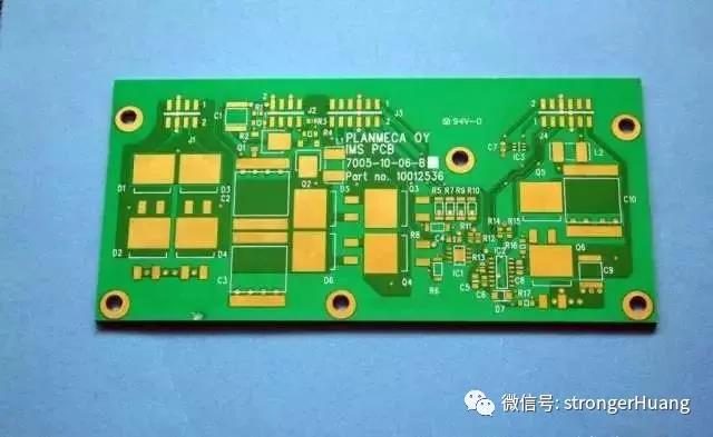
How the two finishes compare
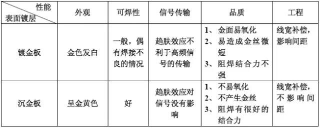
The most consequential differences for a hardware team are summarized here:
- Thickness and appearance: ENIG gold is generally thicker than electroplated gold, and the color is more yellow. The two deposits form different crystal structures.
- Solderability: ENIG is easier to solder and less prone to solder defects. Electroplated gold is harder and more wear-resistant, which is why gold finger boards typically use it.
- Where the gold sits: On an ENIG board, nickel and gold appear only on the exposed pads. The signal travels in the copper layer beneath the solder mask, so at high frequency the skin effect keeps the current in the copper and the finish has little influence on signal integrity.
- Oxidation resistance: The ENIG crystal structure is denser and resists oxidation better than electroplated gold.
- Fine-line routing: As trace width and spacing shrink toward 3–4 mil, electroplated gold can produce gold stringers or bridging between features. Because ENIG is present only on the pads, it avoids this failure mode.
- Solder mask adhesion: With ENIG, the solder mask bonds directly to copper on the trace areas, giving a stronger bond and more freedom in engineering compensation without affecting spacing.
- Flatness and assembly: ENIG provides excellent pad flatness and is less likely to produce the black pad phenomenon after assembly. Its shelf life and flatness are comparable to electroplated gold.
Terminology: ENIG, immersion gold, and flash gold
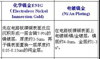
Different regions and companies use different names for the same processes. ENIG and immersion gold (also called chemical nickel gold) refer to the same chemical deposition family, while electroplated gold and flash gold refer to the electrolytic family. The formal names are electroless nickel immersion gold and electroplated nickel gold. The distinction that matters is the deposition mechanism: chemical reduction versus direct-current plating. The table below summarizes the mechanistic difference.
Why lead-free HASL is often avoided for dense boards
As IC integration increases, pin counts rise and lead pitches shrink. Vertical hot-air solder leveling (HASL) struggles to flatten fine pads consistently, which complicates SMT placement and stencil printing. HASL boards also have a relatively short shelf life. Gold finishes address both problems:
- For surface mount assembly, especially 0603 and 0402 passives, pad flatness directly determines solder paste printing quality and therefore reflow yield. Electroplated gold and ENIG are both common in high-density and ultra-small SMT designs.
- During prototyping, boards often wait weeks or months before assembly while components are procured. Gold finishes offer a shelf life many times longer than tin-lead alloy, and at the prototype stage the cost difference is small.
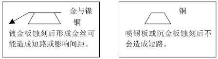
As routing density increases and trace width and spacing reach 3–4 mil, electroplated gold can create gold stringer shorts between features. At the same time, rising signal frequencies make the skin effect more significant: high-frequency alternating current concentrates near the conductor surface, so current traveling through multiple plated layers can affect signal quality. The skin depth depends on frequency, as calculated below.
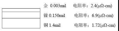
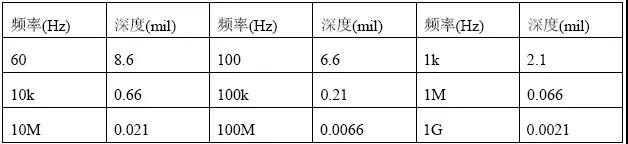
These limitations of electroplated gold are the reason many high-density designs specify ENIG instead.
What this means for your build
- Match the finish to the feature: Specify hard electroplated gold for edge connectors and gold fingers that see repeated insertion, and ENIG for fine-pitch SMT pads, high-density routing, and assemblies that need long shelf life.
- Watch the 3–4 mil threshold: If your trace width and spacing are approaching 3–4 mil, electroplated gold raises the risk of gold stringer shorts; ENIG avoids that failure mode because the gold is confined to the pads.
- Plan for shelf life: If boards will sit in storage for weeks or months before assembly, a gold finish gives you far more margin than lead-free HASL.
- Confirm the deposition method in your fab notes: Because ENIG, immersion gold, electroplated gold, and flash gold are used loosely across the industry, state the mechanism and the target nickel and gold thicknesses explicitly.
- Account for plating bus constraints: Electroplated gold needs a conductive path to every plated feature, which can affect panelization and routing; ENIG does not.
Source: compiled from public web sources.