
High-speed circuit design demands more than a schematic that simulates well. Once signals leave the source and travel across a printed circuit board, every layout decision affects whether the design meets its timing, noise and EMC targets. The seven technical areas below cover the layout issues that most often determine success or failure in high-speed boards.
Power delivery and via placement
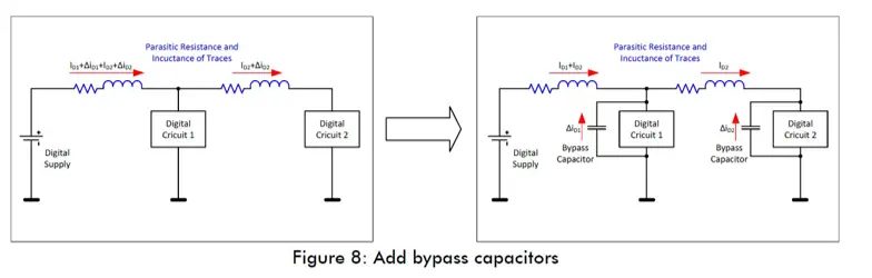
Digital circuits draw current in bursts, so high-speed devices can generate surge currents. When power traces are long, those surges produce high-frequency noise that couples into other signals. High-speed circuits also contain parasitic inductance, resistance and capacitance, so the noise finds paths into neighboring circuitry. Parasitic inductance limits how much surge current a trace can supply, which can cause a voltage drop and potentially make the circuit malfunction.
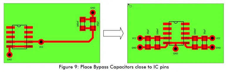
Adding bypass capacitors close to digital devices is therefore essential. Because a large capacitor cannot respond quickly enough at high frequencies, a common practice is to combine a large capacitor with a small one to cover the full frequency range.
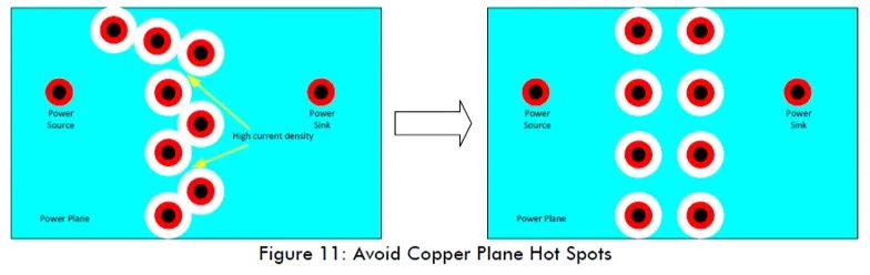
Avoid hotspots. Signal vias create voids in power and ground planes. Poorly placed vias can raise current density in certain regions of a plane, and these high-density areas become hotspots. If a plane is split, return paths lengthen and EMC problems follow. The usual remedy is to place vias in a grid pattern so current density stays uniform and the plane remains continuous.
Trace bends and signal proximity
High-speed traces should run as straight as possible. When a bend is unavoidable, avoid acute or right angles and use obtuse angles instead.
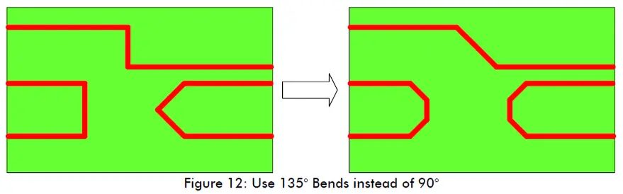
Serpentine routing is often used to match lengths, and it is itself a form of bending. Trace width, spacing and the bend pattern should all be chosen deliberately, with spacing that satisfies the 4W/1.5W rule.
High-speed traces placed too close together are prone to crosstalk. Layout constraints or board outline limits sometimes force spacing beyond the minimum requirement, but where space allows, increase the distance between high-speed traces as much as possible. When a bottleneck forces traces closer, widen the spacing as much as you can near that bottleneck.
Stubs, impedance and differential pairs
A long stub behaves like an antenna and can cause serious EMC problems. Stubs also cause reflections and degrade signal integrity. They most often appear when pull-up or pull-down resistors are added to high-speed lines. A common fix is daisy-chain routing. As a rule of thumb, a stub longer than one-tenth of a wavelength acts as an antenna and becomes a real problem.
Trace impedance depends mainly on trace width and the distance to the reference plane: wider traces have lower impedance. The same principle applies to the pads of connectors and devices. When a large pad connects to a narrow high-speed trace, the pad has low impedance while the narrow trace has high impedance, creating impedance discontinuity and signal reflection.
A common remedy is to place a copper keepout beneath the large pad and add a reference plane on another layer for that pad, raising impedance so it stays continuous. Vias are another source of discontinuity. To minimize the effect, remove unneeded copper where inner layers connect to the via. This can be handled in the CAD tool or coordinated with the PCB manufacturer.
Differential pairs must maintain equal width and equal spacing to achieve the target differential impedance, so route them symmetrically. Do not place vias or components inside a differential pair, as this causes EMC problems and impedance discontinuity.
When series coupling capacitors are required, place them symmetrically and keep packages small. 0402 is recommended, 0603 is acceptable, and 0805 or larger capacitors, or side-by-side capacitors, are best avoided.
Vias create large impedance discontinuities, so minimize their use on high-speed differential pairs. When vias are necessary, place them symmetrically.
Length matching and timing
High-speed interfaces such as buses require attention to arrival time and skew between signal lines. In a parallel bus, all data lines must arrive within a specified skew window so setup and hold times stay consistent. Differential pairs must maintain tight skew or communication may fail. Serpentine routing is the standard way to meet these requirements.
Serpentine routing should be placed at the source of the mismatch, not at the far end. Compensating at the source keeps the positive and negative signals of a differential pair traveling in sync for most of their length.
Bends are one source of mismatch. Length compensation for a bend should be placed close to it, within about 15 mm.
If two bends are separated by less than 15 mm, their mismatches tend to compensate each other, so no additional length matching is needed.
Different segments of a high-speed differential pair should be matched independently. Vias, series coupling capacitors and connector pads split a pair into separate segments, so each segment needs its own matching. Many EDA tools only check total trace length during DRC, so this requires deliberate attention.
Interfaces such as LVDS displays often carry several differential pairs with strict inter-pair timing requirements and very small skew budgets. For these, compensate within the same plane, because signal propagation speed differs between layers.
Some EDA tools include trace length inside pads when calculating length. Compensating based on that number can leave the actual trace mismatched, so verify how your tool measures length.
Whenever possible, route symmetrically from the start to avoid serpentine compensation later. If space allows, add a small loop at the source of the shorter differential line rather than using serpentine routing.
What this means for your build
- Place bypass capacitors close to every high-speed device and combine large and small values to cover the full frequency range.
- Use via grids on power and ground planes to keep current density uniform and prevent plane splits that lengthen return paths.
- Avoid acute and right-angle bends, and keep high-speed traces as far apart as the layout allows to reduce crosstalk.
- Eliminate long stubs, remove unneeded copper at via connections, and keep differential pairs symmetric with minimal vias.
- Match lengths at the source of the mismatch, match each differential segment independently, and confirm how your EDA tool measures trace length before compensating.
Source: compiled from public web sources.